
| Version 2 (modified by , 6 years ago) ( diff ) |
|---|
-
GW16113 miniPCIe Expansion Module
- Features
- I/O pins
-
Customizable Firmware
- Firmware Images
- Firmware Updates
- General Purpose IO (GPIO)
- Universal Asynchronous Receiver Transmitter (UART)
- I2C Interface
- Serial Peripheral Interface (SPI)
- Controller Area Network (CAN)
- Delta Sigma Analog to Digital Converter (ADC_DelSig)
- Sequencing Successive Approximation ADC
- Digital to Analog Converter (DAC)
- On Board LEDs
- Software Support
- PSoc 5LP and Firmware
- Cable and Connector Information
GW16113 miniPCIe Expansion Module
The GW16113 is a miniPCIe expansion module that offers a flexible variety of I/O and function by using a Cypress PSoC 5LP.
The GW16113 is currently under design but we are sharing preliminary specs
Features
Preliminary Specifications:
- miniPCIe form-factor
- miniPCIe socket providing PCIe signalling and USB signalling pass-through
- 3x 10pin Port connectors:
- 1x 3.3V power pin
- 1x ground
- 8x I/O (24 total) 3.3V TTL with various termination configurations
- USB FS interface to host processor
- on-board USB hub (to provide USB pass-through to miniPCIe socket)
- 2x surface mount green user-controllable LED's
Gateworks will offer the GW16113 pre-programmed with a specific firmware configuration. Preliminary Specifications:
- 8x GPIO (8 pins) with configurable modes
- 2x UART (2 pins: TX, RX) (No RS232)
- 1x I2C master/multi-master/slave (2 pins: SCL, SDA)
- 1x SPI master (3 pins: MISO, MOSI, SCLK)
- 1x CAN controller (3 pins: TX, RX, TX_EN)
- 1x ADC (1 pin: 20-bit Delta Sigma)
- 1x ADC (1 pin: 12-bit Successive Approximation (SAR))
- 2x DAC (2 pins: Configurable waveform generation, voltage or current source/sink)
- 2x LED (no external pins)
I/O pins
Thw 24 I/O terminals available on the GW16113 are 3.3V TTL level
Pin I/O details:
- Voltage
| Parameter | Description | Min | Max | Comment |
|---|---|---|---|---|
| VGPIO | Range of Input Voltage | -0.5V | 3.8V | VSSD-0.5 to VDDD+0.5 |
| VMIN | Maximum Input voltage | 3.8V | VDDD+0.5 | |
| VIH | Input voltage high threshold | 2.31V | - | 0.7 x VDDIO |
| VIL | Input voltage low threshold | - | 0.99V | 0.3 x VDDIO |
| VOH | Output voltage high | 2.9V | - | VDDIO-0.4 |
| VOL | Output voltage low | - | 0.8V | IOL = 25mA |
- See CY8C58LP datasheet section 11.4 for more details
- Current capabilities
| Parameter | Description | Source | Sink | Notes |
|---|---|---|---|---|
| IGPIO | J2/P3,J1/P0 current | 4 mA | 8 mA | |
| ISIO | J1/P12 current | 4 mA | 25 mA | 1 |
- See CY8C58LP datasheet Figure 11-8 and 11-9 for GPIO (J2/P3 and J1/P0) output curves
- See CY8C58LP datasheet Figure 11-10 and 11-11 for SIO (J1/P12) output curves
- The GW16113 has 332 ohm series termination resistors between the PSoC pins and the external connectors limiting the current to 10mA - contact sales@… for information on creating a Gateworks special with modified termination
Customizable Firmware
Multiple pre-built firmware configurations may be available for download here.
Users can also choose to customize the firmware on their own to suit their needs. The Gateworks PSoC Creator source is available here. The Cypress PSoC Creator is the free Windows development tool provided by Cypress used to design and compile firmware for PSoC devices.
The GW16113 uses the CY8C58LP (part number: CY8C5888LTI-LP097) from the PSoC5LP family which has the following:
- 32bit ARM Cortex-M3 CPU with 32 interrupts
- 24-channel DMA controller
- 24-bit 64-tap fixed-point digital filter processor (DFB)
- 256KB program flash
- 64KB RAM
- 2KB EEPROM
- Digital peripherals:
- 4x 16bit timer, counter and PWM blocks
- 1x I2C controller (up to 1mbps speed)
- 1x USB 2.0 Full-Speed (FS) (12mbps) (not available for use - this is how we communicate to the host processor)
- 1x CAN 2.0b (16rx / 8tx bufers)
- 20 to 24 universal digital blocks (UDB) programmable to create any number of functions:
- 8-, 16-, 24-, and 32-bit timers, counters and PWMs
- I2C, UART, SPI, I2S, LIN 2.0 interfaces
- CRC blocks
- Pseudo random sequence (PRS) generators
- Quadrature decoders
- Gate-level logic functions
- Programmable clocking
- Analog peripherals:
- Configurable 8- to 20-bit delta-sigma ADC
- 2x 12-bit SAR ADCs
- 4x 8bit DACs
- 4x comparators
- 4x opamps
- 4x programmable analog blocks to create:
- Programmable gain amplifier (PGA)
- Transimpedance amplifier (TIA)
- Mixer
- Sample and hold circuit
- Cypress CapSense support
- 1.024V +/- 0.1% internal voltage reference
- LCD direct drive from any GPIO
References:
Firmware Images
The current firmware images available from Gateworks here are:
- GW16113_HID_GPIO - Vendor-ID/Product-ID: 0x2beb:0x1110 - beta - current factory default
- GW16113_Composite Vendor-ID/Product-ID: 0x2beb:0x1113 - coming soon
The firmware resides in the 256KB PSoC FLASH therefore is non-volatile and contains both the bootloader as well as the main application. See below regarding firmware updates.
Firmware Updates
The PSoC has 256KB of programmable non-volatile FLASH that are used to contain the 'firmware application'. The pre-built firmware images provided by Gateworks contain a PSoC5 Bootloader application that allows for USB updates of the main application (aka bootloadable) firmware.
GW16113 bootloader details:
- Bootloader is programmed at the factory via JTAG and is not able to be updated via USB (technically an application firmware can be created that allows updating the bootloader however Gateworks does not currently support this)
- USB Vendor-ID and Product-ID of bootloader: 0x2beb:0x1100
- Bootloader application is run when GW16113 comes out of reset (when PCI_RESET# is released) and will do one of the following depending on EEPROM configuration:
- remain in the bootloader awaiting a command (to jump to existing app, or program new app)
- remain in the bootloader awaiting a command if the state of the I/O ports latched coming out of reset matches a predefined value, otherwise jump to the application immediately
- jump directly to application
- main application can be instructed to jump to the bootloader and wait for a command (to allow firmware updating)
Options 1 and 2 above are designed to provide a fool-proof way of recovering from a failed firmware update, or faulty firmware that does not allow a method to jump back to the bootloader.
The factory default configuration is to stay in the bootloader a logic value of 0x55 (pin1,3,5,7 logic high, pin2,4,6,8 logic low) is latched on P12 (J1) when the GW16113 comes out of reset (option 2 above).
The bootloader configuration is stored in the PSoC EEPROM and can be altered via the gwsoc application (or directly by the main application if using custom firmware) if the default configuration does not suit your needs.
The gwsoc application running on the host processor has the ability to instruct the application to jump to the bootloader and await a command for updating the main application firmware. The '-p' command-line option is used to update the firmware providing a '.cyacd' file.
Examples:
- program GW16113_HID-GPIO firmware:
wget http://svn.gateworks.com/gwsoc/gw16113/GW16113_HID-GPIO.cyacd
gwsoc -p GW16113_HID-GPIO.cyacd
If for some reason the use case demands the 15KB FLASH space (of 256KB available) used by the bootloader or the ability to update the firmware via USB is not desired, the firmware can be customized by the user to eliminate the bootloader. The resulting firmware would need to be programmed via JTAG. Contact sales@… if this is a requirement.
General Purpose IO (GPIO)
The I/O pins allows a variety of Drive Modes:
- strong drive
- open drain, drives high
- open drain, drives low
- resistive pull-up (5.6kOhm typ)
- resistive pull-down (5.6kOhm typ)
- resistive pull up/down (5.6kOhm typ)
- high impedance digital
- high impedance analog
Several GPIO's will likely be able to be configured with different capabilities:
The USB API will allow the following:
- get/set I/O direction (input/output)
- get/set digital logic level
- set digital logic level
- configure power-up pin drive mode
Reference:
Universal Asynchronous Receiver Transmitter (UART)
The Universal Asynchronous Receiver Transmitter (UART) Component Features
- 9-bit address mode with hardware address detection
- Baud rates from 110 to 921600 bps or arbitrary up to 4 Mbps
- RX and TX buffers = 4 to 65535
- Detection of Framing, Parity, and Overrun errors
- Full Duplex, Half Duplex, TX only, and RX only optimized hardware
- Two out of three voting per bit
- Break signal generation and detection
- 8x or 16x oversampling
The PSoC 5LP does not have fixed hardware UART blocks but instead uses resources from the UDB array.
The USB API will allow the following:
- read/write data
- configure data communications
Note that there are no transceivers on the GW16113 therefore all signalling is 3.3V TTL level and if RS232 signalling is necessary an RS232 transceiver would be needed off-board.
Reference:
I2C Interface
The I2C component supports I2C slave, master, and multi-master configurations. The I2C bus is an industry-standard, two-wire hardware interface developed by Philips. The master initiates all communication on the I2C bus and supplies the clock for all slave devices.
The I2C component supports standard clock speeds up to 1mbps and is compatible with I2C standard mode, fast mode, and fast mode plus devices as defines in the NXP I2C-bus specification.
Features:
- supports slave / master / multi-master and multi-master-slave operation
- 2 pin standard I2C bus
- supports standard data rates of 100 / 400 / 1000kbps
The PSoC 5LP has 1 fixed hardware I2C block and can provide additional I2C components via UDB blocks.
The USB API will allow the following:
- read/write data
- configure data communications
Reference:
Serial Peripheral Interface (SPI)
The Serial Peripheral Interface (SPI) Master component features:
- 3 to 16bit data width
- four SPI operation modes
- bitrate up to 18mbps
The PSoC 5LP does not have a fixed hardware SPI master interface but instead uses resources from the UDB array. There is both a SPI Master component and SPI Slave component available but the default configuration for the GW16113 will support the master.
The USB API will allow the following:
- read/write data
- configure data communications
Reference:
Controller Area Network (CAN)
The Controller Area Network component has the following features:
- CAN2.0A and CAN2.0B protocol implementation, ISO 11898-1 compliant
- Programmable bit rate up to 1 Mbps at 8 MHz (BUS_CLK)
- Two-wire or three-wire interface to external transceiver (Tx, Rx, and Enable)
- Extended hardware message filter that covers Data Byte 1 and Data Byte 2 fields
- Programmable transmit priority: Round Robin and Fixed
Note that the GW16113 does not have a CAN transceiver. The external pinout will be 3.3V TTL and a CAN transceiver and termination would need to be available off-board.
The USB API will allow the following:
- read/write data
- configure data communications
Reference:
Delta Sigma Analog to Digital Converter (ADC_DelSig)
The Delta Sigma Analog to Digital Converter (ADC_DelSig) has the following features:
- Selectable resolutions, 8 to 20 bits
- Eleven input ranges for each resolution
- Sample rate 8 sps to 384 ksps
- Operational modes:
- Single sample
- Multi-sample
- Continuous mode
- Multi-sample (Turbo)
- High input impedance input buffer
- Selectable input buffer gain (1, 2, 4, 8) or input buffer bypass
- Multiple internal or external reference options
- Automatic power configuration
- Up to four run-time ADC configurations
The USB API will allow the following:
- start/stop conversion
- read ADC value
- select input buffer gain
Reference:
Sequencing Successive Approximation ADC
The Sequencing Successive Approximation (SAR) ADC component provides a 12-bit successive approximation with conversions up to 1M samples per second and a signal to noise ratio better than 70dB.
Features:
- selectable resolution (8, 10, 12 bit)
- selectable sample rate (up to 1 Msps)
The USB API will allow the following:
- start/stop conversion
- read ADC value
- configure resolution and samplerate
Reference:
Digital to Analog Converter (DAC)
The 8-Bit Waveform Generator features include:
- Supports standard and arbitrary waveform generation or static voltage driven or current source/sink value
- Arbitrary waveform may be drawn manually or imported from file
- Output may be voltage or current, sink or source
- Voltage output can be buffered or direct from DAC
- Hardware selection between two waveforms
- Waveforms may be up to 4000 points
- Predefined sine, triangle, square, and sawtooth waveforms
The USB API will allow the following:
- start/stop output
- configure waveform (with 4 to 4000 sample points)
- configure drive mode and speed
- select current or voltage mode
Reference:
On Board LEDs
There are two on-board LED's that can be turned on or off.
The USB API will allow the following:
- enable/disable LED
Software Support
The following is preliminary information and is subject to change
There are two pieces of software dealing with the GW16113:
- The GW16113 firmware that is flashed onto the PSoc chip
- The userspace program that controls the GPIOs, etc
Linux Userspace Utilities
gwsoc
Gateworks will provide a gwsoc command-line utility which will make use of the popular open-source and cross-platform HIDAPI and libusb libraries for:
- updating firmware (the firmware dictates the feature matrix for the I/O pins)
- accessing the various features (ie configuring GPIO's etc).
The gwsoc application will come pre-installed on the various Gateworks Board Support Package (BSP) firmware images. Source-code is also provided (see building gwsoc)
The gwsoc application currently is what is used to get/set GPIO configuration using 32bit registers mapped as follows on the GW16113:
| bit | PSoC Port / Pin | GW16113 |
|---|---|---|
| 0 | P12.0 (SIO) | J1.1 |
| 1 | P12.1 (SIO) | J1.2 |
| 2 | P12.2 (SIO) | J1.3 |
| 3 | P12.3 (SIO) | J1.4 |
| 4 | P12.4 (SIO) | J1.5 |
| 5 | P12.5 (SIO) | J1.6 |
| 6 | P12.6 (SIO) | J1.7 |
| 7 | P12.7 (SIO) | J1.8 |
| 8 | P3.0 (GPIO) | J2.1 |
| 9 | P3.1 (GPIO) | J2.2 |
| 10 | P3.2 (GPIO) | J2.3 |
| 11 | P3.3 (GPIO) | J2.4 |
| 12 | P3.4 (GPIO) | J2.5 |
| 13 | P3.5 (GPIO) | J2.6 |
| 14 | P3.6 (GPIO) | J2.7 |
| 15 | P3.7 (GPIO) | J2.8 |
| 16 | P0.0 (GPIO) | J3.1 |
| 17 | P0.1 (GPIO) | J3.2 |
| 18 | P0.2 (GPIO) | J3.3 |
| 19 | P0.3 (GPIO) | J3.4 |
| 20 | P0.4 (GPIO) | J3.5 |
| 21 | P0.5 (GPIO) | J3.6 |
| 22 | P0.6 (GPIO) | J3.7 |
| 23 | P0.7 (GPIO) | J3.8 |
| 24 | unused | |
| 25 | unused | |
| 26 | unused | |
| 27 | unused | |
| 28 | unused | |
| 29 | unused | |
| 30 | P2.0 (GPIO) | D7 LED (read-only) |
| 31 | P2.1 (GPIO) | D8 LED (read-only) |
Example usage:
- show usage:
# gwsoc
GWSoC Utility v1.00
usage: gwsoc  [-p filename] [gpio[=val]] [gpiodir[=val]] [config<n>[=<val>]]
- program GW16113_HID-GPIO firmware:
# gwsoc -p GW16113_HID-GPIO.cyacd
- get gpio direction register:
# gwsoc gpiodir
GWSoC Utility v1.00
GWSoC_HID: 0x2beb:0x1110 Gateworks Corporation GW16113_HID_GPIO 660070
gpiodir=0x00ffffff
- the value of 0x00ffffff (bit0-23 set) indicate that all I/O's are configured for input
- set gpio direction register (set bit for input, clear for output):
# gwsoc gpiodir=0x00ff00ff
GWSoC Utility v1.00
GWSoC_HID: 0x2beb:0x1110 Gateworks Corporation GW16113_HID_GPIO 660070
gpiodir=0x00ff00ff
- the value of 0x00ff00ff (bit0-7,16-23 set) configures P12 (J1) and P0 (J3) as inputs and P3 (J2) as outputs
- set gpio data register (set bit to drive high, clear to drive low)
# gwsoc gpio=0x00005500
GWSoC Utility v1.00
GWSoC_HID: 0x2beb:0x1110 Gateworks Corporation GW16113_HID_GPIO 660070
gpio=0x00005500
- the value of 0x00005500 indicates to drive P3.0,2,4,6 cooresponding to J2.1,3,5,7 logic high
- get gpio data register:
# gwsoc gpio
GWSoC Utility v1.00
GWSoC_HID: 0x2beb:0x1110 Gateworks Corporation GW16113_HID_GPIO 660070
gpio=0x00005500
- the value of 0x00005555 indicates that P12.0,2,4,6 cooresponding to J1.1,3,5,7 are reading high (these are inputs per the gpiodir setting above) and P3.0,2,4,6 cooresponding to J2.1,3,5,7 are outputing logic high
Building gwsoc from source
To build the gwsoc application on an Ubuntu Linux host:
git clone http://github.com/Gateworks/gwsoc
cd gwsoc/gwsoc
sudo aptitude install libudev-dev libusb-1.0-0-dev libhidapi-dev # install dependencies
make
You may also want to install a udev rule to allow group ownership of hid devices for the plugdev group:
# cat /etc/udev/rules.d/99-hid.rules
KERNEL=="hidraw*", SUBSYSTEM=="hidraw", MODE="0664", GROUP="plugdev"
Linux Device Drivers
Linux native kernel drivers will be provided in the Gateworks Board Support Packages (coming soon).
PSoc 5LP and Firmware
The GW16113 is based upon the Cypress PSoC 5LP device which is a programmable device which can be best thought of as cross between a microcontroller combined with a PLD and programmable analog. This means that the board can operate in many different modes depending on how it is programmed.
References:
- PSoC 5LP Product page
- PSoC5LP CY8C58LP Family Datasheet
- PSoC5LP Component list
- PSoC5LP Architecture Technical Reference Manual (TRM)
PSoC Resources and Capabilities
Cypress provides pre-configured functional blocks referred to as 'Components' that can be supported by the PSoC. Conceptually these are virtual peripherals that each have their own datasheet, schematic library representation, and support code implementing an API.
The Cypress PSoC Creator is the free Windows development tool provided by Cypress used to design and compile firmware for PSoC devices. To create firmware that can be programmed on a PSoC you use this tool to drag-and-drop and configure schematic representations of components and edit ANSI-C code to configure and control the components.
A list of components compatible with the PSoC 5LP is available from Cypress PSoC5LP here and all of these are available within PSoC Creator.
Each PSoC 5LP has a fixed set of internal resources available such as:
- RAM
- FLASH storage
- Univeral Design Blocks (UDB)
- Digital clock dividers
- Pins
- DMA channels
- Comparators
- Programmable Analog Blocks
- Interrupts
- various Fixed blocks (ie USB, CAN, I2C, SPI, UART, controllers)
Each component has its own individual datasheet that contains details such as:
- Features
- Software API
- Hardware configuration info
- Resource usage
To determine what can fit into a PSoC you can compare the PSoC datasheet list of resources with the individual component datasheets. Preferably PSoC Creator can generate a resource summary by:
- Workspace Explorer -> Results Tab -> Select the usage report file titled <project-name>.rpt
- Build -> Generate Project Datasheet (refer to section 2)
Cypress also has a nifty online tool that knows quite a bit about what each component needs and what is available. It is used for selecting a PSoC chip but can also be useful to prove that your basic needs can be met. You can find their epsg tool here. Note that this tool does not take into account that we only have 24 I/O pins available to connectors.
References:
Programming PSoc Firmware
- Compile the firmware using the PSoc creator detailed above
- Copy the file to the Gateworks SBC board that has the GW16113 installed
- Verify the gwsoc software is accessible via the command line on the Gateworks SBC
- Verify the USB code is still present in the new firmware image as this code is used to access and update the PSoc and without it, the board could be bricked.
- Program the firmware to the GW16113 with the program flag in the gwsoc application
gwsoc -p {filename}
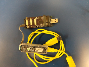
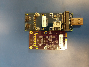
Cable and Connector Information
Cables are sold seperately.
Attachments (2)
-
cypress16115.jpg
(44.8 KB
) - added by 5 years ago.
cypressand16115
-
1611516113.jpg
(44.2 KB
) - added by 5 years ago.
16115and16113
Download all attachments as: .zip