
| Version 1 (modified by , 3 years ago) ( diff ) |
|---|
Venice Digital IO
The intent of this page is to provide information about Venice single board computers general purpose off-board digital IO signals.
DIO and pin function Mapping
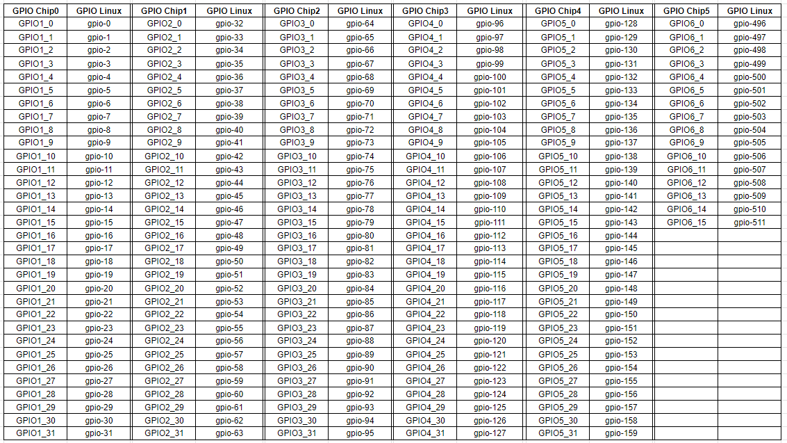
Venice baseboards provide multiple digital IO signals to a connector. The IMX8MM has 5 GPIO blocks having 32 GPIO's each which typically get mapped to gpio 0 - through gpio 159 in the Linux kernel. Note that this mapping is not guaranteed to stay the same across kernel versions - you can look at the debugfs /sys/kernel/debug/gpio file to see where the IMX8MM GPIO controller is mapped.
The various Venice product hardware manuals contain a table of what pins on the Digital IO connector routes to what IMX8MM GPIO. In some cases these signals can be pinmux'd internally to other functions as indicated in the table.
See the operating manual "Specifications", "Electrical" section for information on DIO max and min driving strength.
Venice DIO Mapping:
| Board | Connector | Primary Function | IMX8MM_PAD | GPIO | Notes |
|---|---|---|---|---|---|
| GW730x/GW720x | J9.1 | DIO0 | GPIO1_IO07 | gpio7 | |
| J9.2 | DIO1 | GPIO1_IO09 | gpio9 | can be ENET1_1588_EVENT0_OUT3 | |
| J9.3 | UART1_RX | GPIO5_IO24 | gpio152 | shared with GPS RX | |
| J9.4 | UART1_TX | GPIO5_IO23 | gpio151 | shared with GPS TX | |
| J9.5 | I2C3_SCL | I2C3_SCL | gpio145 (GPIO5_IO17) | shared with MIPI connector | |
| J9.6 | I2C3_SDA | I2C3_SDA | gpio147 (GPIO5_IO19) | shared with MIPI connector | |
| J9.7 | GSC_ADC1 | - | - | Can measure 0 to 5V | |
| J9.8 | GSC_ADC2 | - | - | Can measure 0 to 5V | |
| J9.9 | VDD_3P3 | - | - | ||
| J9.10 | GND | - | - | ||
| GW710x | J25.1 | VDD_5P0 | - | - | |
| J25.2 | GND | - | - | ||
| J25.3 | VDD_5P0 | - | - | ||
| J25.4 | GND | - | - | ||
| J25.5 | VDD_3P3 | - | - | ||
| J25.6 | GND | - | - | ||
| J25.7 | SPI_MOSI | ECSPI2_MOSI | gpio139 (GPIO5_IO11) | can be UART4_TX3 | |
| J25.8 | SPI_MISO | ECSPI2_MISO | gpio140 (GPIO5_IO12) | ||
| J25.9 | SPI_SCLK | ECSPI2_SCLK | gpio138 (GPIO5_IO10) | can be UART4_RX3 | |
| J25.10 | SPI_SS0 | ECSPI2_SS0 | gpio141 (GPIO5_IO13) | ||
| J25.11 | I2C3_SCL | I2C3_SCL | gpio146 (GPIO5_IO18) | can be PWM4_OUT1 | |
| J25.12 | I2C3_SDA | I2C3_SDA | gpio147 (GPIO5_IO19) | can be PWM3_OUT1 | |
| J25.13 | UART3_RX | UART3_RXD | gpio154 (GPIO5_IO26) | ||
| J25.14 | UART3_TX | UART3_TXD | gpio155 (GPIO5_IO27) | ||
| J25.15 | GSC_PB# | - | - | Connect pushbutton to GND | |
| J25.16 | GSC_ADC1 | - | - | Can measure 0 to 5V | |
| J25.17 | DIO0 | GPIO1_IO07 | gpio7 | ||
| J25.18 | DIO1 | GPIO1_IO09 | gpio9 | can be ENET1_1588_EVENT0_OUT3 | |
| J25.19 | DIO2 | SAI1_RXD1 | gpio99 (GPIO4_IO3) | ||
| J25.20 | DIO3 | SAI1_RXD2 | gpio100 (GPIO4_IO4) |
- This is the signal name from the Venice hardware manuals
- This is the connector pinout.
- requires modifying the device-tree to change the pinmux
Note that all signals (unless noted in notes) are 3.3V tolerant.
Note that any GPIO can be used for the following:
- an additional SPI chip-select for those boards that have a SPI bus connector
- a 'bit-banged' PWM (using CPU timers)
- a 'bit-banged' I2C bus (using CPU timers)
- a 'bit-banged' MDIO bus (using CPU timers)
Useful links
Attachments (1)
-
gpio.png
(86.4 KB
) - added by 5 months ago.
updated chart
Download all attachments as: .zip